Jonathan Feasby

Finalising Component Parts

I have locked in the requirements for optical readout, optical addressing, optomechanics, and the surrounding magnetic field. I have cost estimates and supplier links for all of these parts, I have also discovered that CAD models of these parts are available for download online. This saves a great deal of time over my previous method of making the CAD from scratch.

There are a few sections left to fill out on the document which I will fill in tomorrow surrounding operating environment, software control and assessment criteria, then I can do a final price analysis and build the CAD system itself.

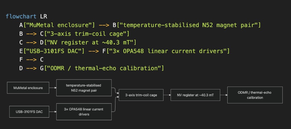
Flowchart of magnetic field control: MuMetal enclosure and temperature-stabilised N52 magnets feed a 3-axis trim-coil cage driven by a USB-3101FS DAC and OPA548 current drivers, setting the NV register at about 40.3 mT for ODMR and thermal-echo calibration.

Specifying is Difficult

The vision of the computer that's floating around in my mind is starting to take a more well-defined shape. I've split the component parts out into function boxes; that is to say, light generation and manipulation is one box, the diamond plate and metallisation is another box, RF/MW generation is another and optomechanics is another still. I am beginning to develop a better geometric intuition for how these boxes are put together to create a full system.

That said, there are far, far more component pieces than I had previously assumed. Mounts (the things that hold the component parts in place) take up a large percentage of this number, as do all the fiddly connecting parts: wires, optical fibre and the like.

Have been somewhat derailed by my rejection from Entrepreneurs First, but am reassured by my current reading of Churchill: Walking with Destiny by Andrew Roberts. When Churchill was my age he was captured while fighting in the Second Boer War, and made an escape from a prisoner of war camp then travelled around 300 miles to friendly territory. In comparison my hardships seem somewhat meek.

Specify!

In interviews of Steve Jobs and Edwin Land, both mentioned that during the design process they could see the finished product right there in their heads, and the only difficulty was getting it down onto paper.

Today my vision for what the diamond computer looks like came to me — vague and ill-defined as it may still be.

Aside from this I have made some good progress on outreach. Diatope replied and confirmed they can handle 14N implantation, annealing, NV characterisation, and identification of suitable single-NV registers. Pricing/lead time still pending.

John Martinis, winner of the 2025 Nobel Prize in physics, agreed to a call on quantum manufacturing on Monday. If my EF experience has taught me anything it's that I shouldn't jump the gun with celebrations, but even getting a response from a Nobel laureate is pretty cool.

Semiconductors to Systems

Attended a conference in London today for people working in and around semiconductor technology. I made some useful connections with whom I will follow up soon, including:

  • Dr. Simon Thomas, CEO of Paragraf (a graphene electronics manufacturer) who invited me for a tour of Paragraf production facilities.
  • Dr. Neil Curson, a professor of nanotechnology and nanofabrication at UCL, currently working on silicon spin qubits. He mentioned having fabrication facilities that can place particles with a 2-atom-wide precision. Will be calling with him on Tuesday.
  • Dr. Joe Smith, lecturer in quantum technologies at the University of Sheffield. His research regarding photonic interconnects between solid-state defects is extremely relevant; we have arranged a lab visit on the 21st of September.

A small note on general 'vibe', there was (with the exception of those people listed above) something of a sense of defeatism and low energy in a lot of the talks given at the event. A clear, non-meandering and optimistic communication style is key to differentiation in such environments.

Back to the drawing board

The immediate goal is a complete blueprint for a small NV-centre diamond quantum computer including the architecture, manufacturing plan, and a bill of materials.

Figuring that if one is to build a computer, one must first have a blueprint for a computer, I’ve spent the day working through the physical machine piece by piece: diamond substrate and NV creation, microwave/RF delivery, control electronics, optics and readout. I’ve contacted Element Six about the diamond plate itself, Ionoptika and Diatope about NV creation, and started evaluating an RFSoC4x2 running QICK-DAWG as a lower-cost control system (I looked at something from Quantum Machines but they cost around $150k, while an RFSoC4x2 is about $3k and QICK-DAWG is free).

I also received the news from Entrepreneurs First that I would not be making it into the FALL26 cohort. This is of course a setback (not to mention embarrassing given that I'd already told my friends that I'd already gotten in), but whatever. Upon hearing the news I got the first train down to London to protest my case in person, but upon my arrival they had all gone home already. I went back the next morning too but to no avail. I am concerned that I rubbed someone up the wrong way, and that this was what led to my being kicked off the program.

Their main objections were that I hadn’t demonstrated that I could recruit strong people and that I appeared too committed to one idea. I disagree with parts of that assessment, but the recruiting criticism is testable. I need to get excellent technical people interested enough to actually work on this.

I’ve also started publishing some of the work I've been doing. I posted the earlier ion-trap design on Hacker News and have started self-advertising in the comments section of 632nm to try get my work in front of a technical audience.